Last Updated on 07/31/2018 by Chris Gampat
Interestingly, we got a fun fact from Canon Watch about Nikon designing its sensors. Hands up if you’re among those who haven’t heard of it yet!
Newsflash: Nikon designs its own sensors. If you’re just hearing about this for the first time, don’t worry; you’re most likely one of many. Canon Watch was another (so you’re in good company), leading to a blog post sharing some details about how Nikon exactly is involved in the making of its sensors.According to the blog post, the short story is that Sony manufactures the sensors but it’s Nikon that designs them. The former is something the photography community is more familiar with, but the latter, especially how deep Nikon is involved with the sensor design, is the news maker here. To get into the details, Canon Watch followed the adventures of Imaging Resource’s Dave Etchells into Nikon’s “super-secret sensor design laboratory.”
Much to Etchells’ surprise (and now our own), there’s actually a deep process involved:
Companies designing chips of whatever sort generally rely on standard processes established by the “foundry” company that does the actual manufacturing. In these cases, the design process is “just” a matter of defining the layout of the devices on the chip. I say “just” though, because it’s far from a routine process to do this. The size and shape of transistors, photodiodes, resistors and capacitors determines their electrical characteristics, and there are loads of tradeoffs involved in balancing light-gathering efficiency, noise levels, readout speeds, on and on. A big trick is designing the pixels and readout circuitry so there’s as little “dead” (non-light-sensitive) area as possible, while maintaining readout speeds and minimizing power consumption.
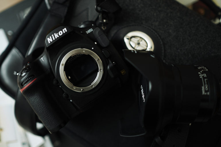
Etchells adds that Nikon puts a lot into the sensor design apart from all the simulations and testing in order to be “able to optimize the system as a whole, in ways that you can’t if you’re just using off-the shelf parts.” With this, their sensors will be optimized for their lenses and work hand-in-hand with Nikon’s in-house designed EXPEED image processing engine. We best see the results of this meticulous processes involved in sensor design, testing, and simulation in the Nikon D850 and D5 sensors.
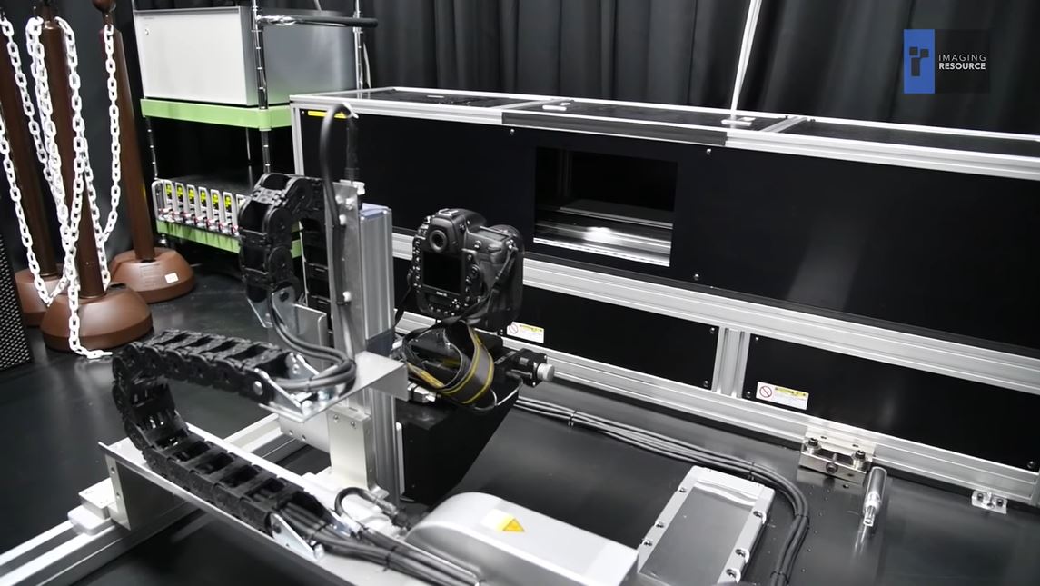
The video below by Imaging Resource shows what goes into one of these tests:
Screenshot image from the video by Imaging Resource; from where this is a sponsored post


